
North East Wafers is developing 300mm silicon wafers engineered for advanced semiconductor fabrication. Our facility is designed with a target capacity of 475,000 wafers per month at full ramp.
Product Lines
The figures below are indicative engineering targets under development and subject to change as our qualification process progresses. Please contact us to start a technical conversation.
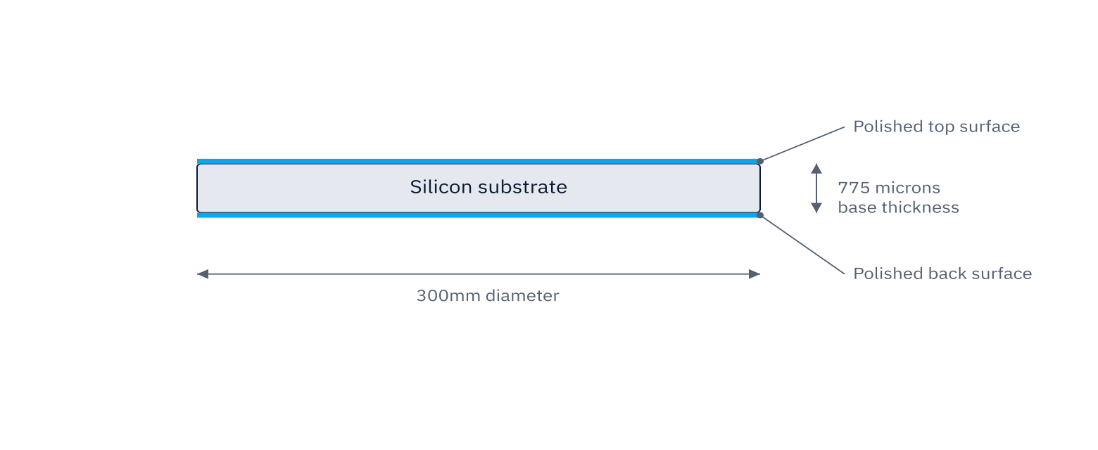
Prime Polished Wafers
Double-side polished 300mm wafers manufactured to conform to SEMI M1 (Specification for Polished Single Crystal Silicon Wafers), covering dimensional, electrical, and surface quality requirements for front-end device fabrication.
| Parameter | Target Range |
|---|---|
| Diameter | 300mm |
| Base Thickness | 775 microns |
| Resistivity | 1–100 Ω·cm |
| Total Thickness Variation (TTV) | < 2 microns |
| Bow | < 30 microns |
| Warp | < 30 microns |
| Surface Roughness (Ra) | < 0.2 nm |
| Particle Density (≥0.12µm) | < 0.1 particles/cm² |
Epitaxial Wafers
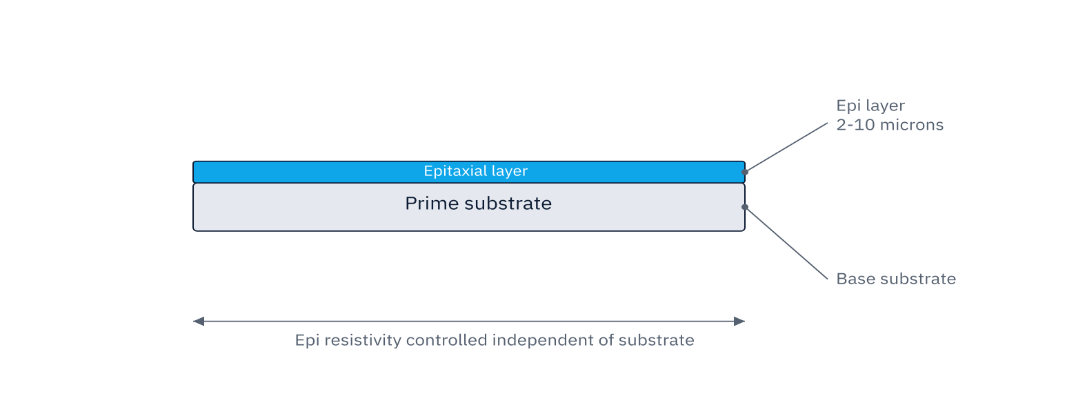
Prime wafers with a controlled epitaxial silicon layer deposited on the surface, conforming to SEMI M62 (Specification for Epitaxial Wafers), offering precise resistivity and defect control for high-performance device layers.
| Parameter | Target Range |
|---|---|
| Diameter | 300mm |
| Epi Layer Thickness | 2–10 microns |
| Epi Layer Thickness Uniformity | < 2% |
| Epi Layer Resistivity | 1–50 Ω·cm |
| Surface Defect Density (LPD, ≥0.12µm) | < 0.1 defects/cm² |
Argon-Annealed, COP-Free Wafers
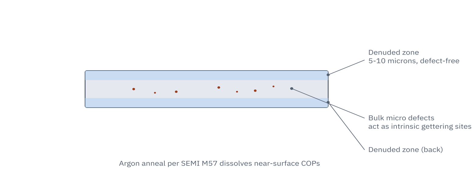
Wafers annealed in an argon atmosphere in accordance with SEMI M57 (Specification for Silicon Annealed Wafers), reducing crystal-originated particles/pits (COP) near the surface and forming a denuded zone for applications where near-surface defectivity must be minimized. This denuded-zone-plus-bulk-defect architecture is a standard, well-established approach used across the wafer industry for defect-sensitive applications.
| Parameter | Target Range |
|---|---|
| Diameter | 300mm |
| Denuded Zone (DZ) Depth | 5–10 microns |
| Surface COP Density | < 0.05 defects/cm² |
| Bulk Micro Defect (BMD) Density | 1×10⁸–1×10⁹ /cm³ |
Interested in learning more about our capabilities? Get in touch.

